| Sign In | Join Free | My himfr.com |
|

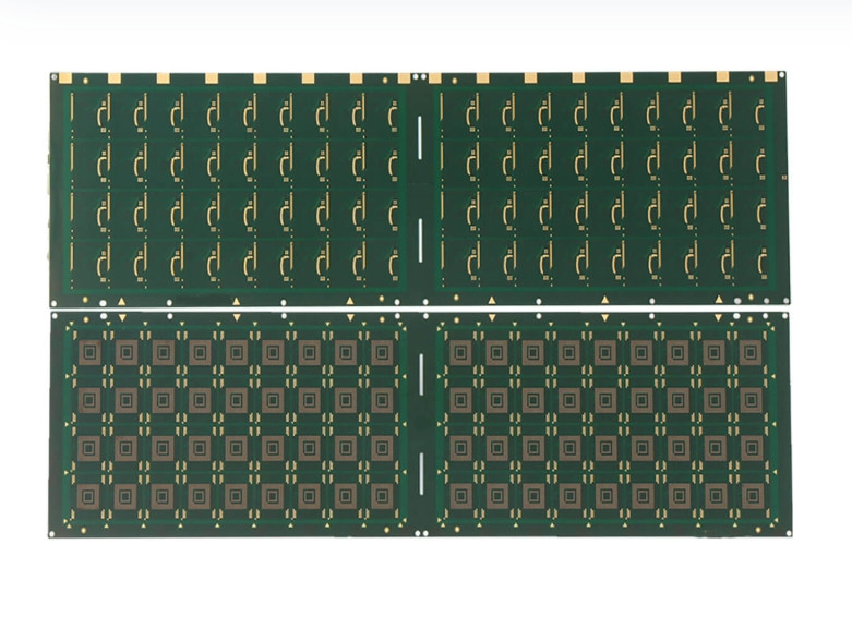
Shenzhen Tecircuit Electronics Limited
Your Vision ,Our circuit , Your Trusted Partner in PCB and PCBA solutions.
Verified Supplier
1 Years
- Home
-
Products
- Multilayer PCB(11)
- Industrial Control PCB Assembly(42)
- HDI PCB(15)
- Consumer Electronics PCB Assembly(87)
- Quick Turn PCB Assembly(18)
- Rigid Flexible PCB(25)
- 2 Layer PCB(13)
- Communication PCB Assembly(19)
- Automotive PCB Assembly(30)
- FPC Flexible PCB(12)
- High Frequency PCB(9)
- Gold Finger PCB(11)
- Metal Core PCB(28)
- IC Substrate PCB(6)
- Ceramic PCB Board(6)
- About Us
- Quality Control
- Contact Us
- Get Quotations